Black silicon nanotextures offer significant optical performance improvements when applied to crystalline silicon solar cells. Coupled with conventional pyramidal textures, to create so–called hybrid black silicon, these benefits are shown to be further enhanced. Presented here is a comprehensive analysis of different variations of this texture, coupled with typical anti–reflectance schemes such as coated pyramids, with a view to the significance of this on subsequent, real–world, solar energy generation. The study uses an angle–resolved spectrophometry system to characterise and compare the optical properties of these surface textures in terms of reflectance versus wavelength and incident angle, with and without encapsulant layers. This analysis, coupled with time-resolved, location specific irradiance data, leads to a new figure-of-merit, the weighted reflectivity, with which to compare surface textures for use in solar cells. Weighted reflectivity for an encapsulated solar cell surface, averaged over a year, for a Southampton, UK, location is calculated to be 7.6% for hybrid black silicon, compared to 10.6% for traditional random pyramids with a thin film anti–reflective coating.
Introduction
The nanoscale texturing of crystalline silicon (c-Si) solar cells, naturally dubbed ‘black silicon’ (b-Si) for its resultant appearance, has been subject to considerable research interest in recent years [1–4]. This is primarily due to the significant gains in optical performance offered with its use, with more light being absorbed into the substrate for subsequent electron-hole (e-h) pair generation. The methods used to create such textures vary from reactive ion etching (RIE) [5], to metal-assisted chemical etching (MACE) [6], and femtosecond laser (FsL) surface treatments [7]. For RIE and MACE methods, the resultant surface consists of vertically–aligned nanowires (NWs) with properties dependent on a large variety of factors including etch time, chemical composition, and temperature [8]. For FsL texturing, surface structure is dependent on pulse energy, duration, and angle of incidence [9,10]. The optical benefits of b-Si can be further enhanced when the texturing process is applied to microscale textures such as random pyramids [4] - a standard anti–reflectance texture used in monocrystalline silicon photovoltaics (PV). This combination of micron-scale pyramids decorated with nanoscale b-Si features is termed “hybrid b-Si” (hb-Si).
Black silicon does not interact with electromagnetic (EM) radiation in the same fashion as its microscale counterparts [11]. Pyramidal textures, for example, exhibit relatively good anti-reflectance arising from their ability to direct initially reflected light, that would otherwise be lost, onto adjacent facets for a second or third chance of being coupled into the solar cell. Furthermore, the redirection of light away from the normal means that reflected light escaping the surface is more likely to undergo total internal reflection at the overlying encapsulant interfaces and be redirected back onto the cell. Light trapping within the cell is also enhanced by the texture as the inclined facets change the propagation direction of transmitted light through refraction, increasing the optical pathlength and therefore the amount of light absorbed. Pyramidal texturing is often combined with a thin film anti–reflection layer which operates through a destructive interference mechanism to further lower the reflectance of light at the silicon interface [12]. Nanoscale textures, such as b-Si, lead to a graded refractive index between the substrate and surrounding medium, smoothing the transition of light from one medium to the other and hence minimising reflectance over a broad spectral and angular range.
The measurement and quantification of optical performance for samples of applicability to solar PV is a crucial determinant in their effectiveness for use in such systems. We explore the application of MACE b-Si, applied to planar and pyramidal–textured substrates, and compare against the industry standard, microscale pyramids with a single–layer anti–reflectance coating. Optical performance is defined using front surface reflectance as measured with an in-house designed and constructed angle–resolved spectrophometry (ARS) system. A detailed description of the ARS can be found in our previous publication [13]. A new perception of these anti–reflectance schemes is showcased, enabling a more thorough analysis that includes variations in reflectance with both wavelength and angle of incidence. Other than simply observing the relation between the reflection from a surface of a solar cell and its angle dependency, it is shown that variable angle reflectance (VAR) data captured by the ARS can be related to the surface optical response to a moving source over time: the Sun [14]. Taking solar irradiance for a specific geographical location, and transient daylight hours for the same across a given year, the angle–dependant reflectance can be converted to to time– and seasonal–dependant reflectance, extrapolating anticipated optical performance of the surface design when it is applied to a PV cell. This leads to a single optical figure of merit; the weighted reflectivity (WR), which can be used to compare different anti–reflective schemes.
Experimental Methodology
Four types of samples were fabricated for characterisation: a standard random pyramidal texture using an anisotropic potassium hydroxide (KOH) based chemical etch, the same with an 80 nm SiNx single–layer ARC, several b-Si nanotextures of various heights using a MACE procedure [15,16], and hb-Si nanotextures, also of various heights, through a sequential series of KOH and MACE processes. The b-Si samples used here have etch times of 4, 6, 8, and 10 minutes, yielding mean NW heights of between 1.09 and 2.55 𝜇m, respectively. As for the hb-Si samples, only the former three etch times were used, as a 10 minute MACE process on top of the random pyramids caused excessive deterioration of the microscale texture. The average heights of these hb-Si textured NWs for 4, 6, and 8 minute MACE were 0.79, 1.17, and 1.61 𝜇m, respectively. Scanning electron micrographs of each textured sample can be seen in Fig. 1.
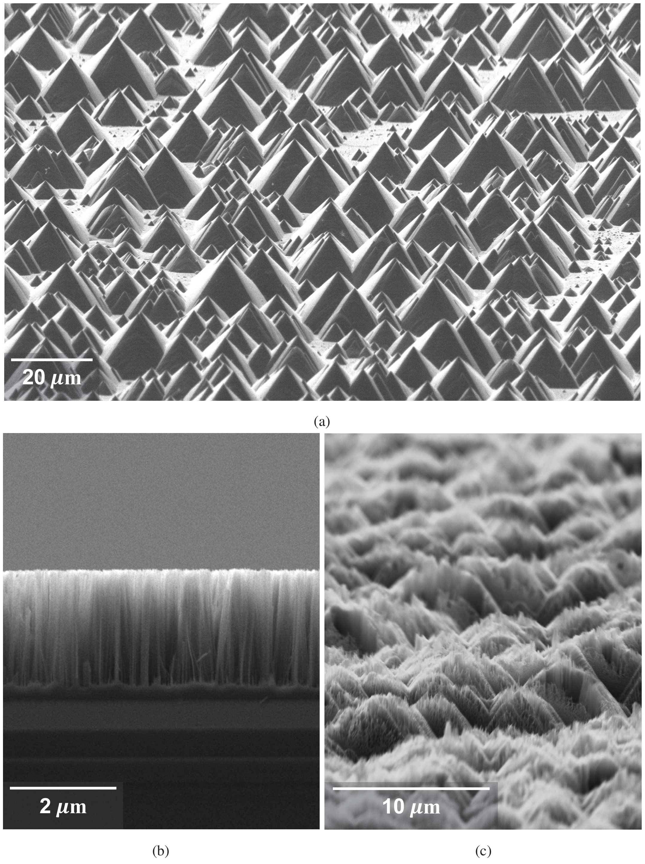
Figure 1: Scanning electron micrographs of exemplar pyramidal (a), planar b-Si (b), and hb-Si (c) textures used in this work.
The ARS is used to perform high resolution centre–mount VAR scans on these nine samples, with a diffuse reflectance standard of 50% used as a reference. The ARS technical specifications and operational modes are outlined in [13], but the scan parameters used in this work were: 𝜆=400:1000 nm, 𝜃=8:80∘, where S– and P–polarisations were averaged together over five consecutive scans.
Subsequent to these measurements being taken, two of the best performing samples are then encapsulated in Norland Optical Adhesive (NOA) 61 [17] and 1.5 mm thick borosilicate glass. NOA 61 offers >95% transmission of light between wavelengths of 400 nm and 1.8 𝜇m – covering the range of interest explored using the ARS system and completely covering the typical operating range of Si–based solar cells, and is a very close match to the performance of EVA, a commonly used adhesive in module production. The NOA 61 encapsulant layer is applied in the centre of each 3×3 cm sample, ensuring coverage does not exceed half the area of that sample. The borosilicate glass layer is then placed on top of this, causing the NOA 61 encapsulant to spread across the sample surface underneath the glass for complete surface area coverage. Samples were cured in an ultraviolet light irradiance box for a period of one minute, in–line with the manufacturer’s specifications. Prior to completing any optical measurements, the encapsulated samples were inspected to confirm the absence of any visible air bubbles. It should be noted that this glass does not include its own ARC, and, as a result, front surface reflectance reported forthcoming for these samples may be slightly higher than those with this additional glass ARC. Such a coating is common in production modules, and improves optical performance, but is not explored here.
Data analysis and methodology
In order to understand the process by which VAR data can be related to real–world equivalent scenarios, we first need to evaluate how the Sun moves relative to the solar panel over the length of the solar day, i.e. the proportion of a 24 hour period where the Sun is above the horizon. The solar day length is affected by several factors, such as specific geographical location, the height of the terrain above sea level (elevation), and whether the location is in the northern or southern hemisphere. The change in solar elevation throughout the year can be visualised by taking the two solstices (shortest and longest days of the year); all days in–between will have solar elevations situated between these two curves.
Solar elevation data is calculated using NREL’s solar position algorithm (SPA) [18]. For this work, the parameters used in the SPA are tailored for Southampton, UK, having geographic coordinates of 50∘ 54′ 9.126″ N (latitude) and 1∘ 24′ 15.0804″ W (longitude), with an elevation of 2 m. Even when the Sun is below the horizon, light can still reach the solar panel indirectly. As such, negative values of elevation, that is to say when the Sun is below the horizon, are only included in situations whereby the SPA indicates a significant component of scattered light throughout the atmosphere. Month–dependent cloud coverage was included as part of this calculation, with coverage values provided by the Met Office [19] over a 10 year period.
Using spectral irradiance data, weighted average reflectance can be determined for a given sample. In typical, single angle reflectance measurement systems, this weighted average reflectance (WAR) is a single figure of merit weighted against the AM1.5G spectrum [20] to provide a more valuable insight into the true reflectance implications for solar PV technologies. WAR is determined for single angle reflectance as shown in Eq. (1), where 𝑅𝑥 is the sample’s surface reflectance, 𝜆 is wavelength, and 𝐹AM1.5 is the AM1.5G spectral irradiance curve [20].
\[\text{WAR}=\frac{\int[R_x(\lambda)F_{\text{AM1.5}}(\lambda)]d\lambda}{\int[F_{\text{AM1.5}}(\lambda)]d\lambda}\]