This work explores the implications of random and non-linear nanostructures on electromagnetic wave propagation, within a multiphysics simulation environment. Showcased is a way to noticeably bypass the inaccuracies drawn from the linearity dependency of traditional simulation methods. Applying the COMSOL Multiphysics software platform, the finite element method and a geometry expanded-on from previous work, the analysis of highly intricate nanostructured material surfaces is uniquely reported.
Introduction
Whilst research within materials science turns increasingly toward the nanoscale, with electronics following suit, there is a more pressing concern regarding our ability to simulate such materials with a sufficient degree of accuracy. Take for example black silicon (b-Si), a silicon surface textured with nanoscale features to minimise reflectance of light [1-3]. Notably, b-Si has a very low broadband reflectance spectrum due to its unique light scattering properties. The physics behind this high level of anti-reflectance essentially hinges on the fact that the nanoscale surface features present here are far smaller than the wavelength of light incident on it. This means that ray-tracing in the geometric optics regime cannot be used to accurately model these textures.
Unfortunately, an accurate method of simulating such heterogeneous nanoscale surfaces and their subsequent interaction with electromagnetic (EM) waves remains hard to come by. Several methods have been explored previously, including effective index techniques (EIT) [4] and the finite difference time domain (FDTD) method [5]. The application of the finite element method (FEM) in this work enables a new level of geometric manipulation that, with the appropriate use of statistical mathematics, intricate meshing strategies and generation sequences, permits the simulation of b-Si surfaces to a higher level of accuracy within a computational physics environment.
The geometry
Employed within the core component of this model is the COMSOL®† Wave Optics module configured to provide EM wave injection in the frequency domain, opposing the use of the time domain for shorter simulation run time and greater resource efficiency. A wavelength domain study step is used in conjunction with a cluster sweep setup to utilise the University of Southampton’s IRIDIS 5 supercomputer for rapid multi-parallel computation capabilities1.
The model used here is an extension on previous work by the author, and not taken from any of the application libraries. It was designed using two types of material domain; one of air and the other of silicon. The silicon and air domains were placed against each other such that a single interface was formed between them. Perfectly matched layers (PMLs) were then employed to extend these domains infinitely away from the interface between them. A 4 × 4 square grid of b-Si nanowires (NWs) could then be created at this interface, extruding outward from the silicon into the air. The air domain was elongated automatically to ensure complete encapsulation of all the NWs within the grid using global parameters. The boundaries parallel to the z-axis were configured with Floquet periodicity conditions to ensure the domain could be replicated across both the x and y axes.
To create stochastic nanostructures, certain functions with seeded inputs needed to be created to randomise individual parameters of these NWs, such as radius, height, bend and pitch. This meant that no pair of NWs could be the same. It is noted how electronic systems can never be truly random and, as such, artificial randomness, or pseudorandomness, needed to be generated for each of these parameters. Using random function and logical switch definitions built into COMSOL Multiphysics R©†, along with certain mathematical expressions and static parameters, pseudorandomness on a per-NW basis could be achieved for the first time at this level of complexity.
Our results have demonstrated thus far that, by simulating many unit-cells of these random NWs, and then taking an average of their EM reflectance, a far more accurate spectral response can be obtained when compared to that of a real, truly random b-Si surface on which the model was based [6]. The implication is that we can now, far more accurately, simulate heterogeneous nanoscale surfaces whilst also being able to vary the average properties of the aforementioned surface to identify the global effects on its spectral response characteristics. This is extremely useful for the creation of anti-reflective surfaces for a broad range of applications.
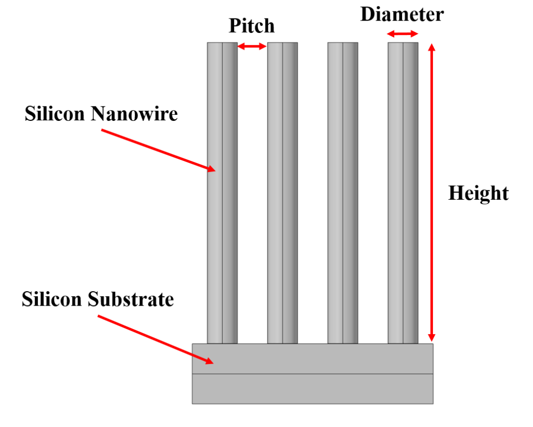
Figure 1: Diagram showing side-on view of silicon nanowires defined in the simulation, with the key properties labelled.
There are five key properties that needed to be randomised here: NW pitch, height, radius, bend/bunching and form. Figure 1 shows graphically the three former properties, whilst the two latter will be explored separately. Using a series of random functions set with a uniform probability distribution, a randomisation sequence was created for each property. Another was created to randomise the other random functions by generating a different seed for each; this formed a two-layer pseudorandomisation sequence for each property. Each property was given a static input value, for example a height of 1 μm, and subsequently some degree of variation was applied to that number separately for each NW created. The maximum variation was defined as a percentage of the static input. In this example, a maximum variance of 10% would permit the height of any individual NW to lie somewhere between 0.9 and 1.1 μm. The variance values used here were selected as being 7.5%, 15% and 30% for NW height, pitch and radius respectively.
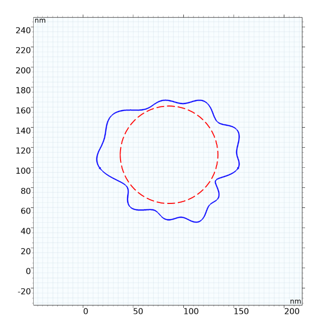
Figure 2: Schematic showing how a random geometric form in nanowire cross-section is generated on a per-nanowire basis using a randomised parametric curve superimposed onto the statically defined nanowire radius.
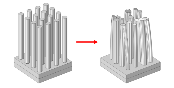
Figure 3: The nanowire simulation geometry with homogeneous (left) and heterogeneous (right) structures.
The form of each NW was generated in a different fashion to the other properties. Parametric curves were drawn randomly, with unity radius, onto a 2-dimensional work plane geometry component superimposed onto the substrate surface in the 3-dimensional domain. An example of such a curve is shown in figure 2. Following this, convert-to-solid (CTS) methods were applied to turn the curve into an enclosed surface, which could subsequently be extruded from the surface in the 3-dimensional domain. Nanowire bunching is created through the use of a virtual ‘bunching zone’, drawn at the top of each parametric curve. A random function determines a factor by which each NW is influenced towards this zone, and subsequently to some degree towards one another. Any NW that lies outside of this zone are left with a random degree of bending in any given direction. This is demonstrated in figure 4.
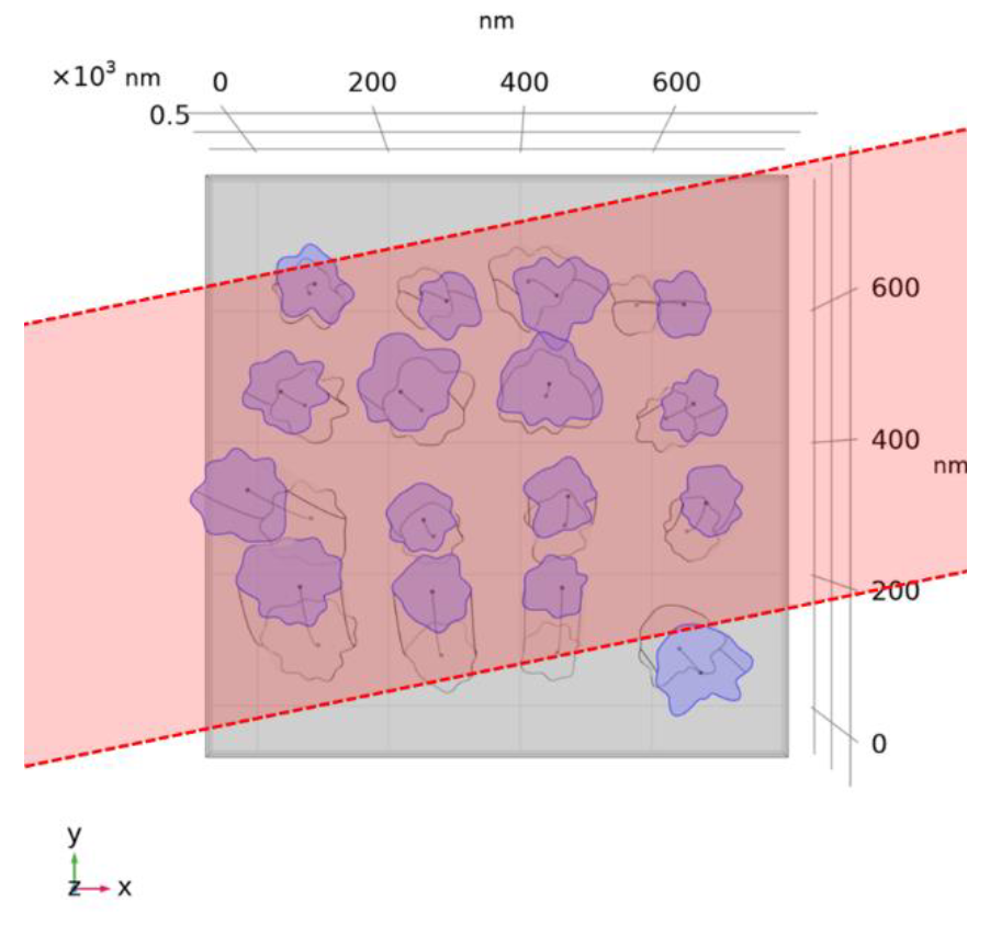
Figure 4: A demonstration of the virtual ‘bunching zone’, as well as how it influences encompassed nanowires. Note how the bottom right nanowire, lying outside of this zone, is not influenced towards the others.
Methodology
The simulations reported here were run on the IRIDIS computer cluster1. As a result, the solver was configured to use both a cluster sweep and a nested parametric sweep. The nodes within the cluster computer lacked any graphics processing units (GPUs), and as a result rendering a geometry using one of these nodes would be an inefficient use of simulation resources and time. Instead, each geometry was rendered locally on the host machine, before being sent to the cluster on a per-seed basis. No further geometric changes were applied during the simulation process, given that the nested parametric sweep carried out a wavelength sweep only.
To ensure the accuracy of our results, and to overcome the issues associated with using Floquet periodicity for heterogeneous geometries, we needed to simulate several different random geometries and take an average of their results. This simulation methodology has been explored previously in work by Altermatt et al. [7]. The minimum number of different geometries required to achieve convergence in the results needed to be found. Once this value was known, an identical number of different input seeds for the geometry can be added to the simulation file in the form of a parametric sweep.
The electromagnetic wave, frequency domain interface was employed with two ports configured within the domain. One of these ports injected an electromagnetic wave and measured the intensity of the wave reflected backwards from the silicon substrate.
Results and discussion
A convergence study in the averaging of the results from simulations of multiple random geometries was first carried out. Figure 5 shows the cumulative reflectance data from the first 50 different input seeds. It is clear from this data that, below a value of 37 iterations making up the cumulative average reflectance, convergence is not achieved, and the data is highly unstable. However, past this point, the reflectance value settles at 3.5% ± 0.1%. For efficiency, it is not worth simulating above this number of geometries given the negative effect on the runtime of the simulation model.
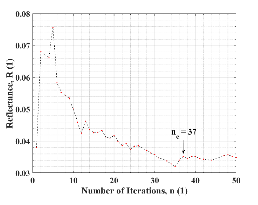
Figure 5: Plot of simulated average reflectance for 700 nm wavelength light vs. number of iterations included in the averaging, demonstrating convergence after averaging the reflectance of 37 geometries.
Figure 6 shows the data, taking the value of n_c = 37 forward, for a broadband averaged reflectance sweep of 𝜆 = 400 − 1000 nm in steps of 25 nm. Also plotted is the experimentally-measured reflectance spectrum from a black-silicon surface with NW heights of approximately 1 μm [6]. Plotted in red are reflectance values extracted from each of the 37 individual simulations, with the average of these plotted as a dashed line.
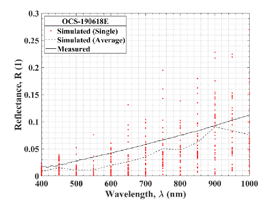
Figure 6: Reflectance simulations of 1 μm high nanowires, and measured data of comparable manufactured equivalents.
There are several key points to note from the data shown in figure 5. Primarily, the average reflectance matches well to that of the measured reflectance. Average broadband reflectance values for the simulated and the measured data are 4.14% and 5.99%, respectively. It is also clear to see how the diversity in the individual reflectance simulations is far greater towards the larger wavelengths, whilst those in the 400 – 600 nm range vary far less. It is possible to deduce that, because of this characteristic, the value of nc may not be constant across all values of λ; the implication here being that fewer iterations need to be averaged to see convergence at these lower wavelengths. Referring to the data shown in figure 4, our convergence study was based on 700 nm wavelength light. It is possible that n_c may be higher above this wavelength, and lower below it. However, by using nc = 37, the convergence for the mid-sweep wavelength, we are ensuring that the point of convergence is not too low for the higher wavelengths, but also not excessively high for the lower ones as this would extend simulation runtime considerably.
Differences between the measured and simulated data may come from slight variances between the properties of the model geometry and the real sample. It is difficult to quantify certain properties of a real sample with absolute certainty – for example the amount the height, radius or pitch of each NW can vary. In this case, observations were made of the sample through SEM images, and variances were estimated. This approach can easily introduce slight errors into our study and is likely the cause of the 1.85% discrepancy between the two sets of data in this case.
Conclusions
Here we have shown an effective method of simulating large-area, stochastic nanostructures using COMSOL Multiphysics®† and the finite element method. By splitting such random geometries up into smaller unit-cells, applying randomisation to each and averaging their individual spectral response, we get a response not too dissimilar to experiment. This opens interesting possibilities in the modelling of other stochastic media for applications other than that explored here.
References
[1] S. K. Srivastava, D. Kumar, P. K. Singh, and V. Kumar, ‘Silicon nanowire arrays based “black silicon” solar cells’, in 2009 34th IEEE Photovoltaic Specialists Conference (PVSC), 2009.
[2] Yung-Jr Hung, Kai-Chung Wu, San-Liang Lee, and Yen-Ting Pan, ‘Aligned silicon nanowire arrays for achieving black nonreflecting silicon surface’, in IEEE Winter Topicals 2011, 2011.
[3] T. Rahman, R. S. Bonilla, A. Nawabjan, P. R. Wilshaw, and S. A. Boden, ‘Passivation of all- angle black surfaces for silicon solar cells’, Solar Energy Materials and Solar Cells, vol. 160, pp. 444–453, Feb. 2017.
[4] T. Rahman and S. A. Boden, ‘Optical Modeling of Black Silicon for Solar Cells Using Effective Index Techniques’, IEEE Journal of Photovoltaics, vol. 7, no. 6, pp. 1556–1562, Nov. 2017.
[5] D. Wu, X. Tang, K. Wang, and X. Li, ‘An Analytic Approach for Optimal Geometrical Design of GaAs Nanowires for Maximal Light Harvesting in Photovoltaic Cells’, Scientific Reports, vol. 7, no. 1, Apr. 2017.
[6] J. J. Tyson, T. Rahman, and S. A. Boden, “Optical simulation of black silicon surfaces using geometric randomisation and unit-cell based averaging,” in 15th Photovoltaic Science, Application and Technology Conference, Apr. 2019, pp. 81–84.
[7] P. P. Altermatt, Y. Yang, T. Langer, A. Schenk, and R. Brendel, ‘Simulation of optical properties of Si wire cells’, in 2009 34th IEEE Photovoltaic Specialists Conference (PVSC), 2009.
Acknowledgements
†COMSOL Multiphysics is a registered trademark of COMSOL AB.
This work has been supported by the Centre for Doctoral Training in New and Sustainable Photovoltaics (EPSRC grant number EP/L01551X/1), and completed as part of Black Silicon Photovoltaics (EPSRC grant number EP/R005303/1). The author of this work also acknowledges the use of the IRIDIS compute cluster, and associated support services at the University of Southampton, in the completion of this work.